Germanium has a role in the exciting future of VCSEL-based 3D Sensing Applications

VCSELs (Vertical Cavity Surface Emitting Lasers) were developed in the first years of this century for data communications and industrial sensing applications. The logical substrate of choice was then 4" GaAs. The volumes were low and the VCSEL die size was <1mm². A first big disruption for the VCSEL market was the introduction of the 2017 Apple iPhone with 3D face recognition using VCSELs. And since Apple has deployed a VCSEL based, world facing LiDAR on its iPad and iPhone platforms. Up till now the GaAs supply chain has been able to follow this evolution, shifting from 4" to 6" wafers.
Sabbir Rangwala has published two excellent pieces in Forbes where he looks at the future of these VCSEL based 3D Sensing Applications. Part 1 looks at the market and application drivers in new applications. Part 2 looks how the supply chain is responding to these market drivers and where the best solutions lie.
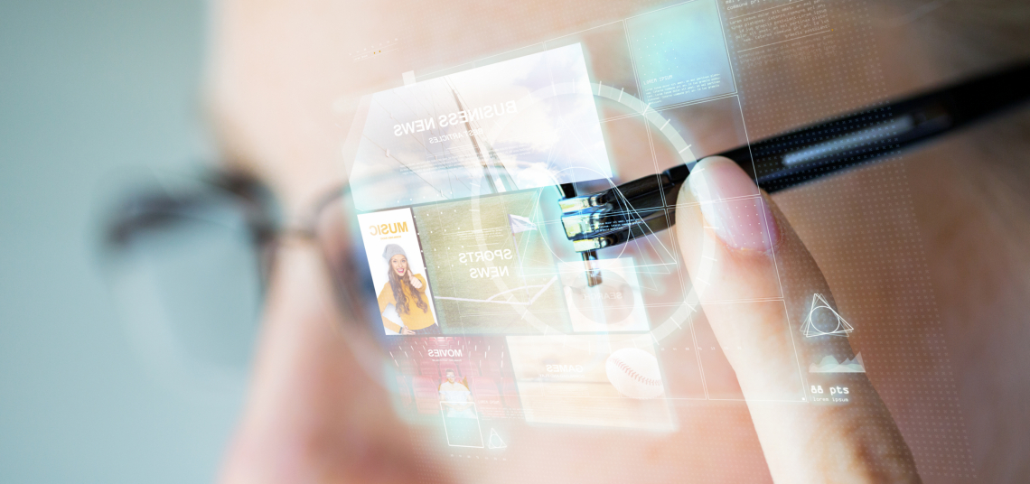
One of the conclusions is that VCSEL-based LiDAR has some exciting future applications. The initial disruption of the VCSELs integration in the iPhone and iPad opens the route to other applications, such as automotive LiDAR, Augmented/Virtual Reality (AR/VR) and emerging smart glasses. These applications would mean a new disruption for VCSEL-based LiDAR.
The question is when, not if.
Sabbir Rangwala, Forbes
Previously the GaAs substrate platform was able to follow the first disruption, although even that was challenging. Not only are GaAs wafers brittle and tend to break more easily, they are also subject to wafer bowing which has an impact on the yields.
This second disruption would demand higher volumes, lower costs, higher performance, different features and more sustainability. For example, there are fundamental differences between cosumer and automotive LiDAR applications, requiring significanly higher levels of performance and reliability. Also, VCSEL arrays in consumer applications tend to be smaller (1-2 mm²), whereas VCSEL based automotive LiDAR uses ~10x larger VCSEL sizes (10-30 mm²).
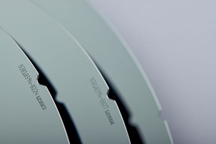
To cope with these challenges, Germanium substrates are emerging as natural choice to for all these challenges. Ge has zero defects (dislocations), lower levels of bow, its thickness can be reduced through selective etching for better thermal transfer, enabling higher VCSEL powers and reliability. Ge wafers are available in 6", but the original Ge wafers market, space solar cells, is ready to make the shift to 8". For VCSELs, shifting to 8" is also the logical next step. There is an estimation of a 5x reduction in VCSEL cost with the transition towards 8" Ge substrates. A shift to 8" Ge also means compatibility with CMOS foundries, enabling high-volume, low-cost integration with driver electronics. Ge is also better suited for longer wavelength operation, which is needed to put 3D sensors behind the OLED screen and more eye safe to increase the power of LiDAR lasers. Finally, the sustainability aspects of germanium are important as the industry ecosystems look to become more environmentally friendly. Umicore Germanium comes mainly from recycling, with most of the rest coming from low carbon footprint germanium sources. Germanium recycling is important, as the GaAs is not recycled, and it doesn't uses toxic Arsenic.
As Sabbir Rangwala concludes: 'The question is when, not if'.
Want more information about Germanium substrates ?
Read more here