The relation between uncooled arrays pixel size and optics in the long-wave infrared
Thomas Hingant, Paul Vervoort, John W. Franks
Article shared under SPIE's Green Open Access Policy
ABSTRACT
Over recent years, the pixel size of uncooled thermal detectors has kept shrinking, going from 50 μm in the last decade to 17 μm today. The latest generation of detectors, with 12 μm pixel pitch and smaller, come with a new set of challenges. In this paper, we investigate the link between pixel size and optics cost and performance by relying on a well-defined framework and concrete examples. First, we briefly clarify the relationship between the reduction in pixel size and requirements on the optics, from both the radiometric and the resolution point of view. Within this framework, we study the effect of decenter corresponding to current state-of-the art manufacturing on performance and price of lenses. Finally we demonstrate that reducing the pixel size indirectly leads to much more demanding lenses. As the new generation of 12 μm pixel pitch arrays are emerging in the long wave infrared, lenses will become more complex and harder to manufacture. Consequently, optics with equivalent levels of performance can become more expensive.
Keywords: LWIR, micro-bolometers, pixel, lens design, tolerances, decenter, cost
1. INTRODUCTION
Since their first appearance, the trend has always been towards smaller pixels for the uncooled micro-bolometers used for long-wave infrared (LWIR) focal plan arrays (FPA). This reduction in size is mostly driven by a desire for a reduction in cost, since the detector contributes the majority of the cost of a LWIR camera. Meanwhile, challenges in reducing the size of pixels are usually tackled from the point of view of the detector[1] and the attention is more towards fabrication, efficiency and filling factor issues.
However, while reducing the pixel size has a strong impact on the detector price and performance, it also influences the lens designs. At the camera level, the user may want to grasp the full implications of using smaller size pixels. Therefore, the description of the optics cannot be limited to a diffraction limited case. In that spirit, this paper will focus on the consequence on actual lens designs for the transition from 17 μm to 12 μm-pixels in uncooled bolometers.
The paper is organized as follows. First, we will define a clear framework for our discussion. We will see that the transition from 17 μm to 12 μm pixels requires faster lenses. Because of this, fabrication errors start to have a much bigger impact on the image quality. We will therefore in a second part focus on one particular error, decenter, and analyze how it impacts a lens design. From this we will indicate ways to build systems that are more robust to fabrication. Finally, we will apply the conclusions previously drawn to the transition from 17 μm to 12 μm pixels, and demonstrate that this transition will lead to much more costly optics.
2. FRAMEWORK – GENERAL CONSIDERATIONS
In discussing the effect of reducing the pixel dimensions, we have to carefully define a framework. There are essentially two ways to use the decreasing size of pixels in a focal plane array (FPA). Either the size of the detector is kept constant and the number of pixels is increased, or the number of pixels is kept fixed, which reduces size of the detector. The latter yields more detectors on a same wafer, which is in principle more cost-effective. Since cost and size seem currently to be the main drivers for reducing the pixel dimensions, we will consider for this study that the number of pixel is kept constant. We will also introduce a supplementary condition to discuss the impact on the optics of a reduction in pixel size. We require that the image formed on the detector remains unchanged, assuming the detector efficiency remains the same. Therefore, we will not take into consideration the possible reduced efficiency of the pixels due to higher electrical noise or reduced filling factor, even though this may also put a strain on the lenses.
First, from the geometric point of view, requiring that the image remains identical on a smaller detector means that the field of view is kept constant, and hence the focal length is reduced. This is illustrated in Figure 1.a and b. In principle, distortion would also have to be the same, but this is so much design dependent that it would be irrelevant to take this into account to draw general conclusions.

Figure 1. Schematic representation of equivalent lenses for a. a 17 μm-pitch detector (designed as FPA) and b. a 12 μm-pitch detector displaying the same number of pixels. H and H’ are the principal planes. The focal length in b. 𝑓12′ has to be reduced to maintain the field of view. If the light collected from an object is kept the same, the diameter of the incoming beam must remain the same and hence the f/# must get faster with the reduced focal length. c. Schematic representation of the intensity distribution of the PSF on the detector with both lenses.
Then, the image must display the same sharpness on a smaller scale. Essentially, this means that the width of the point spread function (PSF) must remain of a size comparable to that of the pixels. Since the width of the PSF is proportional for incoherent light to the diffraction limit unit 𝜆 / NA = 𝜆 ⋅ f/#, scaling the PSF with the pixel size means that the f/# must be scaled accordingly. We have introduced 𝜆 the average wavelength and NA the numerical aperture of the lens. This is illustrated in Figure 1.c. Here we want to stress that changing the f/# is a necessary condition. Another convenient and common way to express the requirement on sharpness is to use the modulation transfer function (MTF) at the Nyquist frequency as a metric. For example, a lens designed for a 12 μm-pixel detector requires the same contrast at 41.7 cy/mm as the one obtained at 29.4 cy/mm by its equivalent, designed for a 17 μm-pixel detector.
Eventually, the same energy from a scene must be collected on the detector. In more rigorous terms, we want the étendue 𝐺 = 𝑆det𝜋 / (f/#)2 to remain constant, with 𝑆det being the surface of the detector (see chapter 4 of the book of Chaves[2]). Under our hypothesis this once again means that the f/# must follow the pixel reduction.
If we summarize, smaller pixel translates into smaller focal length, but also faster lenses. The reduction of the focal length makes it easy to jump to the conclusion that lenses become smaller in size. However, the focal length reduction is directly compensated by the faster f/#. In fact, the entrance pupil and hence the size of the front element of a system would remain the same, provided the image quality is kept constant, as can be seen in the schematic drawing of Figure 1.b. We shall qualify this statement at the end of the paper, since it can be seen that the apertures of lenses in the market do not decrease as fast as the pixels. It can also be true that the rear elements of a system may become smaller, but this is often due to a reduction of the back focal length rather than a reduction of the detector size.
A downside of faster apertures is that they lead to more challenging designs. Aberrations have indeed to be controlled on a bigger solid angle. Although the optical designer can use many tools to tackle this issue, including the use of aspherical surfaces[3], increasing the aperture puts more strain on the optics. With real lenses, what may actually limit the performances is not even the design itself but rather the manufacturing tolerances. These includes deviation from the nominal surface profile, deviation from nominal thicknesses, as well as tilts and decenters of optical surfaces. In the following discussion, we will focus on the example of the decenter of a given optical surface and assess how it constrains the optical design. We will eventually show empirically by means of some design examples that the transition from 17 μm to 12 μm-pitch uncooled FPA in the LWIR requires more complex designs, in order to comply with the current state-of-the art manufacturing techniques.
3. EMPHASIS ON THE MANUFACTURING CONSTRAINTS – CASE OF DECENTER
3.1 Effect of decenter
What we call decenter is illustrated in Figure 2.a. It corresponds to the lateral displacement of the optical surface perpendicularly to the optical axis. The lens design of Figure 2.b is typical of what can be found in LWIR cameras with uncooled bolometers. With the large wavelength, it is easy to fabricate any kind of lens shape[3][4]. Therefore, all surfaces can easily be made aspherical, which allows for a good correction of the aberrations with a very limited number of lenses. In the design of Figure 2.b we have introduced a 10 μm-decenter on the first surface of the rear lens. This is a good order of magnitude of what can happen in making a lens with conventional high volume fabrication techniques in the LWIR. The effect of the decenter on the MTF, at 30 cy/mm, has been computed numerically with a ray-tracing software for different values of the aperture. The result is displayed in Figure 2.c in black whereas the red curve corresponds to the nominal design. First, on the nominal design, we observe that the sharpness increases with faster apertures up to f/1.2. This is simply because at slow apertures, the system is limited in performance by the diffraction. Beyond f/1.2, we can see that the nominal design no longer follows the diffraction limit but rather starts to lose performance, which is the signature of aberrations. This illustrates what was mentioned earlier, that it is more difficult to get to a good nominal design with very fast lenses. More interestingly, the introduction of a decenter representative of LWIR manufacturing techniques does not have any effect on MTF for slower apertures than f/1.4, but then starts to seriously alter the performance beyond f/1.3. Of course, we have only considered one lens surface, but in a real system, all optical surfaces present deviations from the nominal design. Therefore, even if at f/1.1 the nominal lens might have displayed reasonable sharpness, a real lens could see its performance destroyed. Because of this dramatic threshold effect, manufacturing tolerances that were barely noticeable for f/1.4 lenses can become critical at f/1.0. Since the pixel size imposes faster lenses, we will explicitly derive the effect of decenter to understand how it could be reduced.
3.2 Derivation of the wavefront error caused by decenter
To this aim, we will follow the same reasoning than the one presented in chapter 7 of the book of Mahajan[5]. The only difference is that we are not going to constrain ourselves to the case of a decenter in the tangential direction. Our notations are defined Figure 2.a. The direction of the vector decenter Δ is taken to be x. In the unperturbed state, we define the intermediate object as a 2D vector ℎ, and its Gaussian image by the optical surface as ℎ'. The image magnification 𝛾𝑖 is therefore defined as ℎ' =𝛾𝑖ℎ. The object and image in the perturbed state are respectively labelled ℎ𝑝 and ℎ𝑝'. With the introduction of the decenter, we obtain:
ℎ𝑝' = ℎ' − 𝛾𝑖Δ
Thus the dimension of the image in the perturbed state can be approximated far from the axis† by:
ℎ𝑝′ = ‖ℎ𝑝' ‖ =ℎ′ − cos(𝜙)𝛾𝑖Δ + 𝑂(Δ2/ℎ2)

Figure 2. a. Decenter of an optical surface by an amount Δ along the x direction, with a description similar to the one of chapter 7 of Optical Imaging and aberrations by Virendra N. Mahajan[5]. The difference with this reference is that we do not limit ourselves to the case where the decenter is in the tangential plane. The angle between the direction of the decenter and the nominal image is 𝜙. b. Typical lens design for a medium field of view, with an aperture of f/1.0. c. Effect on performance of a 10 μm-decenter on the first surface of the second lens of the design depicted in b., as a function of the aperture. The dashed line indicates qualitatively the limit in f/# beyond which manufacturing defects become more visible.
Now, we can follow exactly the derivation described in chapter 7 of Mahajan’s book[5]. The idea is that the first effect of decenter is to change the paraxial configuration of the system. By using a new set of coordinates corresponding to the shifted optical axis, we just need to determine the transformation from the initial coordinate system without decenter to the new perturbed one. After derivation, we find that the error 𝛿𝑊dec. introduced by the decenter on the optical path difference 𝑊 is given by:
𝛿𝑊dec. = 𝑊(𝑋 − 𝛾𝑝Δ,𝑌,ℎ𝑝′ ) − 𝑊(𝑋,𝑌,ℎ′)
where we have introduced 𝛾p, which is the magnification of the pupil. The error, like in the work of Mahajan[5], is calculated at the new decentered exit pupil. Eventually, by assuming Δ ≪ ℎ, a first order Taylor expansion of 𝑊(𝑋−𝛾𝑝Δ,𝑌,ℎ𝑝′ ) yields‡
𝛿𝑊dec. = −Δ ⋅ (𝛾p 𝜕𝑊/𝜕𝑋 + 𝛾i cos(𝜙)𝜕𝑊/𝜕ℎ′)
There are two terms in equation (1). The term in −Δ𝛾p 𝜕𝑊 / 𝜕𝑋 essentially compares how the wavefront at the pupil resembles itself when shifted by an amount Δ scaled by the magnification. The other term in −Δ𝛾i cos(𝜙) 𝜕𝑊 / 𝜕ℎ′ translates the fact that with decenter the position of an image is slightly shifted in the field by an amount −Δ𝛾i cos(𝜙). Therefore the shifted image gets the optical path of the points located nearby in the field. We also recover the well-known result that every aberration contributes to lower order aberrations in the pupil coordinates due to the term in 𝜕𝑊 / 𝜕𝑋, as well as to the same order aberrations but with a lower order dependence on the field h’ due to the term in 𝜕𝑊 / 𝜕ℎ′. For example, third order coma gets a contribution from third order spherical aberration and third order coma that are both independent of the field. We need to mention as well that in our derivation we assume that after the surface everything is aligned to the new decentered axis. Were it not the case everything can be treated as cascaded decenters, adding each time a similar contribution to the optical path.
As a side comment, by showing that decenter introduces an error on the wavefront, the behavior observed in Figure 2.c becomes obvious. Indeed, if we start with a well corrected system where in the image space 𝑊 ≈ 0, then the error at the exit pupil of the design resulting from a small decenter is directly proportional to 𝛿𝑊dec.. Thus, the image degradation which can be linked to the root-mean-square (RMS) error of the wavefront ∝√∫pupil|𝛿𝑊dec.|2𝜌𝑑𝜌𝑑𝜃 is clearly an increasing function of the aperture. What was not evident at first was that Δ = 10 μm would be a limit value for the system presented in Figure 2.b. This brings us to discuss the possibility to tune the physical parameters in equation (1). This will help us to try and improve the optical quality of as-built systems to get to the 12 μm-pixel requirements.
There are different variables to play with in equation (1). The first term is the decenter Δ. It is of course determined by fabrication techniques. Lower decenters can be achieved by using high-end manufacturing techniques, or even by lens selection. However, the dependence on wavefront is linear in Δ, meaning that substantially reducing the decenter error by fabrication can be extremely demanding and costly. Another option is to assemble lenses to compensate the tolerances, either by pairing lenses with compensating decenters, or by active re-alignments[3]. In any case, this assumes an in-depth knowledge of the system and the need for measurements, which will also be expensive. Therefore, it appears that compensating for decenter at the production level can be considered, but this always comes with a price.
A better strategy may be to reduce upfront the sensitivity of the design. In this case, the terms to play with are the geometrical constants γi and γp, as well as the partial derivatives ∂𝑊 / 𝜕𝑋 and ∂𝑊 / 𝜕ℎ′. We will in the next section discuss two examples showing how one can act on these terms at the design level.
4. REDUCING THE SENSITIVITY TO DECENTER IN THE LENS DESIGN
4.1 Example 1. Thicker lenses
In our first example, we will consider the 18° horizontal field of view (HFOV)-design opened at f/1.1 that is displayed in Figure 3.a. The MTF at the Nyquist frequency for 17 μm is plotted against field height in Figure 3.d, for the nominal design in red, and with a decenter Δ = 10 μm in the tangential direction, on the first surface of the second lens. We observe on the MTF that this decenter strongly affects the performance of the design. Knowing from equation (1) that the sensitivity to decenter of a given surface could be modified by the changing the paraxial combination of powers of each surfaces in a lens design, we have carried out a quick re-optimization in order to loosen the sensitivity on surface 1 of lens 2. The re-optimization has been carried out with the same constraints as in a., for focal length, distortion, and image quality, but without any constraints on envelope, which resulted in a much thicker lens 2. This re-optimized design is presented in Figure 3.b and its MTF versus field with and without decenter is plotted in Figure 3.e, in a similar fashion than for design a. We can observe that the effect on image sharpness of the 10 μm-decenter has completely vanished. This can be explained if we look at Table 1 where we have gathered the values for the image magnification at each optical surface for the designs displayed in Figure 3. For design a, the value of 𝛾𝑖 is of order 1000 at surface 1 of lens 2 while it has been reduced to 𝛾𝑖∼10 in design b, decreasing similarly the sensitivity to the term in ∂𝑊 / 𝜕ℎ′ of equation (1) by two orders of magnitude. Thus, we see that by simply using thicker lenses, the value of the optical surface magnification 𝛾𝑖 can be tuned easily to get rid of overly tight tolerances.
Of course, the design in Figure 3.b is unreasonable because the lens would be too big and heavy, but also therefore expensive. The cost of materials suitable for the LWIR is indeed much higher than the cost of visible glass or plastics, so increasing the thickness of a lens has consequences. Another option in the case of a very thick lens is to split it in two with keeping low power surfaces. This is how we have obtained the design in Figure 3.c. We see in Table 1 that the values of 𝛾𝑖 have been kept low resulting in a design that is still tolerant to decenter. This can be seen on the MTF versus field graph, displayed in Figure 3.f. The sharpness remains the same with and without a 10 μm decenter on surface 1 of lens 2.

Figure 3. a. Original lens design b. Design re-optimized from a., solely to release the sensitivity to decenter of lens 2. c. Design b. where lens 2 has been split, followed with a quick re-optimization with the same constraints. e., f. and d. display the image sharpness with (in black) and without (in red) a 10 μm-decenter on surface 1 of lens 2, for designs a. and b. and c. respectively.
Table 1. List of the image magnifications 𝛾𝑖 for all surfaces in designs a. b. and c. of Figure 3, for an object located at infinity.
| Design | S1-L1 | S2-L1 | S1-L2 | S2-L2 | S1-L3 | S2-L3 |
| a. | 0.00 | 0.87 | 1131.41 | 0.00 | - | - |
| b. | 0.00 | 0.67 | 11.00 | 0.12 | - | - |
| c. | 0.00 | 0.67 | 11.98 | 0.29 | 2.21 | 0.17 |
When looking at the designs of Figure 3, it also appears that the shape of lens 2 looks slightly smoother in design b., and even smoother in design c. This brings us to study the two other terms in equation (1), namely the dependence in the shape of the wavefront 𝜕𝑊 / 𝜕𝑋 and in 𝜕𝑊 / 𝜕ℎ′.
4.2 Example 2. Lower departure from the sphere
In order to discuss the influence of the shape of the wavefront on the sensitivity to decenter, we will try and derive more explicit expressions for the partial derivatives of W. Because the optical systems we consider are in principle of rotational symmetry, it is convenient to decompose the wavefront on the orthogonal basis of Zernike polynomials. For this we will follow the Born-and-Wolf convention[6] and use the elegant un-normalized definition used in the work of Janssen[7]
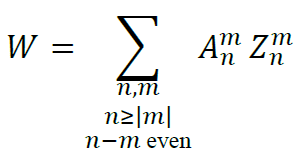
with 𝑍𝑛𝑚(𝜌,𝜃) = 𝑅𝑛|𝑚|(𝜌)𝑒𝑖𝑚𝜃, where 𝜌,𝜃 are the normalized radial and the azimuthal coordinate on the pupil. We will also assume that the decenter is small enough to consider that a decomposition on a circular pupil is still valid. In the case of extreme decenters, strong vignetting would occur that should be taken into account, but this is beyond the scope of this discussion. Using the decomposition on Zernike polynomials and the same notations and conventions than in the paper of Janssen[7], it is straightforward to re-write the expression of 𝛿𝑊dec. in equation (1) and it reads
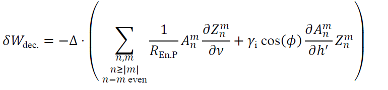
Here we have introduced the normalized pupil coordinates (𝜈,𝜇) = (𝑋 / 𝑅Ex.P,𝑌 / 𝑅Ex.P), and reduced the expression 𝛾𝑝 / 𝑅Ex.P to 1 / 𝑅En.P. 𝑅En.P and 𝑅Ex.P. are respectively the radii of the entrance pupil and exit pupil. If we assume that the decomposition is limited to a finite degree N, and introducing the expression for 𝜕𝑍𝑛𝑚 / 𝜕𝜈 derived in the paper of Janssen et al. it follows that
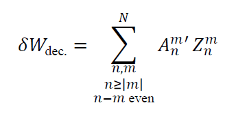
where
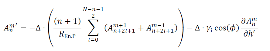
From Parseval’s theorem the variance of 𝛿𝑊dec. is directly proportional to the sum of |𝐴𝑛𝑚′|2/(𝑛+1). Therefore, if the 𝐴𝑛𝑚′ / Δ are big, then the image quality will degrade rapidly with decenter. It is important to notice that terms of higher order n, ie. faster varying aberrations, will have more weight in the decomposition as we can observe that they will have a ∝ (𝑛+1) contribution. Therefore, if W is a badly behaved function in the sense that it is presents important high order terms 𝐴𝑛𝑚, there is a high chance that the effect of decenter will be critical. It is also interesting to remark that the sums in equation (2) make it virtually possible to balance different terms so that for some particular fields 𝛿𝑊dec. vanishes.
By definition, 𝑊 corresponds to the optical path length difference between a reference ray and the rest of the beam. When traversing an optical surface, a phase delay is introduced that is essentially proportional to the product of the index change by the apparent thickness e of the new medium traversed. For example, a collimated beam centered on axis will see a delay ∝(𝑛−1)𝑒(𝜌,𝜃). Therefore, if a surface shows a strong departure from a parabola, in the sense that its thickness profile 𝑒 decomposed on a Zernike basis yields terms in 𝐴𝑛>20 ≫ 𝜆 / (𝑛−1), then it can be expected that the surface will be very sensitive to decenter. Related to this remark, we see here the usefulness of constraining the shape of a lens by its departure from an ideal surface. This once again stresses the importance of using a physically meaningful decomposition for the shape profile, like the one introduced by Forbes[8][9][10].
In Figure 4 we provide a simple illustration to show the actual influence of the waviness of a surface on the sensitivity to decenter. Both designs in Figure 4.a and b have been optimized to produce an image on a 12 μm-pitch VGA (640 x 480), with a horizontal field of view (HFOV) of 75° and an aperture of f/1.0, one with two lenses and the second with three lenses. They display very similar nominal characteristics, although the length of the two lenses-design is slightly longer. However, to get to a good performance with the two lenses-design, extreme aspheres had to be used. As a consequence, the optical path difference created right after the first surface is much bigger for design a. than for design b. With the introduction of a small decenter on the first surface of the front lens, we can see in Figure 4.c and d that the RMS error on the wavefront in the image plane grows much faster for the two lenses-design than for the three lenses-design. This is in agreement with our prediction from equation (2), which we have numerically computed on axis and added as a dashed line if Figure 4.c and d. For a more visual comparison, we have also plotted in Figure 4.e. and f the MTF at the Nyquist frequency without (in red) and with (in black) a 10 μm-decenter along the sagittal plane on the first surface of both designs. The three lenses-design is much more robust to decenter. Eventually, in this particular case, the three lenses-design has proven to be even a more cost-effective solution, this because it is much lighter as well as being more tolerant.

Figure 4. Influence of the departure from sphere on the sensitivity to decenter. a. two lenses-design, and b. three lenses-design giving the same horizontal field of view of 75° on a VGA (640 x 480) with 12 μm-pitch, with the same aperture of f/1.0. c. and d. show for both designs the estimation of ⟨𝛿𝑊dec.⟩, the root mean square (RMS) wavefront error at the exit pupil of the lens introduced by a decenter along the sagittal direction on the front surface of lens 1. The estimation is obtained by subtraction of the wavefront variance with no decenter to the wavefront variance with decenter: ⟨𝛿𝑊dec.⟩=√⟨𝑊dec.⟩2−⟨𝑊0⟩2. This is of course a very crude estimation, but it yields the right order of magnitude and dependence on the decenter Δ. The dashed line correspond to the value of ⟨𝛿𝑊dec.⟩ on axis, computed numerically by summing the squared 𝐴𝑛𝑚′ given in equation (2), with taking cos(𝜙)=1. e. and f. correspond to the MTF computed with (in red) and without (in black) a 10 μm-decenter along the sagittal direction on the surface 1 of lens 1, for both designs shown in a. and b.
With all the degrees of freedom allowed by aspherical surfaces, it is usually possible to find solutions with a very limited number of surfaces. However, not only the final path difference matters, but also what happens in-between the surfaces. It comes to the general and well-known idea that smoothly bending the rays and using not too strong aspherical surfaces leads to much more tolerant designs. As a side remark and before concluding, we would like to point out that even if we have considered only decenter for the sake of conciseness, tilt acts in a very similar fashion. Only the geometrical factors 𝛾i and 𝛾p in equation (1) are replaced by geometrical constants related to the displacement of the pupil and image induced by the tilt. This is for example detailed in the chapter 7 of the book of Mahajan[5]. Thus, all the conclusions drawn with decenter in the previous sections still hold with tilt.
5. IMPLICATIONS OF PIXEL SIZE REDUCTION ON LENS DESIGN
Let us now focus on the 17 μm to 12 μm transition. Typically, optics used with a 17um pixel LWIR FPA will have an aperture in the range f/1.2 to f/1.4. To match this resolution and sensitivity, on a detector with 12 μm pixels, the calculations in section 2 tell us that we will need lenses with apertures in the range f/0.85 to f/1.0. Interestingly, what is mostly found in the market for 12 μm FPA are f/1.0 lenses, so, on the slower side of the range. More generally, apertures of lenses in the market have not changed a lot in the past years, remaining around f/1.2. This is certainly due to the fact that the detectors have improved in sensitivity over time, compensating for the lack in light collection. In the case of diffraction limited optics in the LWIR, resolution is indeed still mostly limited by the detector[1].
Keeping this in mind, we have tried to give a comparison of equivalent optics for both pixel sizes. We have therefore carried out a small design exercise. Using a VGA (640x480) FPA, lenses have been designed with a HFOV ranging from telephoto-8° to wide angle-120°, both for 12 μm and 17 μm detectors. The constraints on these designs were similar. We have looked for highest as-built performance, manufacturability with current fabrication techniques, and designs as light and compact as was reasonable within manufacturability. On the 17 μm detector we have assumed a back working distance > 10 mm to have room to fit a shutter, while on the 12 μm FPA we have assumed that the compactness of the detector would allow a shorter back working distance, typically > 7 mm. With these constraints, we have set equivalent apertures, ranging from f/1.2 to f/1.5 on the 17 μm VGA, and from f/0.8 to f/1.1 on the 12 μm VGA. The layouts of these designs are presented in Figure 5 for the 17 μm-pitch VGA and in Figure 6 for the 12 μm-pitch VGA.
The first point to be noted is that on the 17 μm VGA graph all designs have only two elements, while on the 12 μm VGA graph many designs display three or more elements. The case of the 75°-HFOV f/1.0 lens presented in Figure 4 is therefore not an isolated case. Rather, we can observe that there is a whole region in the 2D space defined by aperture and field of view where two lenses are no longer sufficient. This is, as has been discussed in this paper, a direct consequence of the faster aperture requirement of smaller pixels. Using more than two lenses gives more degrees of freedom to correct the wavefront without introducing large deviations from a sphere. This also make it possible to gradually bend the light rays, without changing the magnification too quickly. All of this contributes to building less sensitive designs and achieving better optical quality. We have indicated by a dashed line on Figure 6 what we consider to be a limit between two and three elements designs. Of course the exact position of this frontier depends on many parameters, such as what is accepted as a good image quality, what are the constraints on envelope, the choice of the detector format, and also the tolerance budget for fabrication. For example, the two lenses-design that we have shown in Figure 4.a could be considered viable, were the decenter accuracy much better than 10 μm. Nonetheless, and with the current state of the art, it is certain that the transition from 17 μm pixels to 12 μm pixels will require more complex designs for wider fields of view. In the same spirit, we even observe that four lenses were necessary to achieve the design of an f/0.8 120° HFOV -lens for the 12 μm-pitch VGA.
Naturally, this transition to more complex designs has a consequence on the cost of the lenses. Our cost estimation is based on many parameters and includes the cost of raw material, as well as the cost of all operations needed to produce the lens. Because a costing model depends on the manufacturer, it is more meaningful to merely compare the relative cost of all designs. We have therefore added the blue dots on Figure 5 and Figure 6. The diameters of these dots represent estimates of the relative cost of each design.
For both detectors, it is first noticeable that narrower fields of view tend to be more expensive. This is simply because a narrow field of view normally requires a long focal length and hence large optics that are expensive to process and consume a lot of material. However, for narrow fields of view (HFOV < 20°), only two lenses suffice to achieve a good image. Therefore, we observe no big change in the cost of a lens when changing the pixel dimension. This is again due to the condition that we have imposed, that the f/# should follow the ratio of the pixel reduction. In the market, for narrow fields of view, f/1.0 lenses sold for the 12 μm pixels are slightly more cost-effective than the f/1.2 counterparts sold for 17 μm pixels, due to the focal length reduction.

Figure 5. Typical lens design space for a 17 μm VGA – diameter of the blue dots are indications of the cost of the lenses

Figure 6. Typical lens design space for a 12 μm VGA – diameter of the blue dots are indications of the cost of the lenses. The same scales have been used than with the designs for 17 μm VGA presented in Figure 5, both for the lens designs and for the costs indications.
With wider fields of view, however, the trend is very different. The necessity to use more than two lenses on the 12 μm pitch-VGA results in big steps in the cost of the lenses. For example, a more than a threefold increase in cost can be expected for a 120° HFOV lens, when shifting from 17 μm pixels to 12 μm. Of course, it is possible that, as for the narrow fields of view, a trade-off on aperture is an acceptable alternative. But even in this case, the cost of wide angle lenses cannot be expected to decrease.
6. CONCLUSION
Overall, the transition from 17 μm pixels to 12 μm pixels in uncooled micro-bolometers FPA presents a new set of challenges. To maintain the image quality, faster and thus more demanding optics are required. We find that the combination of the apertures required by 12 μm pixels and current manufacturing capabilities make it necessary to introduce more complex designs that are more robust to tolerances. We have shown that the introduction of 12 μm pixels will result in an evolution in lens designs for the LWIR. Maintaining the image size and quality will therefore lead to more expensive optics.
As long as the price of the detector remains the main contributor to the cost of a LWIR camera, decreasing the size of the pixels will remain interesting. When this is no longer true, we will see more differentiation in the systems. On the one hand, it will still be possible to obtain even more cost-effective solutions by using smaller apertures. This would result in very affordable compact cameras, with decent but not better image quality. On the other hand, reduction of pixel size could be used with a constant detector dimension, i.e. with bigger detector formats. In such case, because the surface of the detector would remain constant, cameras would not require faster lenses to collect more light. Meanwhile, a bigger sampling of the image by more pixels would offer more ways to apply image post-treatment. This would in the end allow for improving the quality of the images with either a moderate increase or no increase in the cost of the final system.
ACKNOWLEDGEMENTS
The authors would like to thank J. Verplancke, M. Rozé and T. Krekels for their help on this work and for fruitful discussions.
REFERENCES
[1] Rogalski, A., Martyniuk, P. and Kopytko, M., “Challenges of small-pixel infrared detectors: a review,” Rep. Prog. Phys. 79, 046501 (2016).
[2] Chaves, J., [Introduction to Nonimaging Optics], CRC Press (2016).
[3] Braunecker, B., Hentschel, R. and Tiziani, H. J., [Advanced Optics Using Aspherical Elements], SPIE Press (2008).
[4] Parks, R. E., “Fabrication of infrared optics,” Optical Engineering 33(3), 685-691 (1994).
[5] Mahajan, V. N., [Optical Imaging and Aberrations], SPIE Press (1998).
[6] Born, M. and Wolf, E., [Principles of Optics], Cambridge University Press (1999).
[7] Janssen, A. J. E. M., “Zernike expansion of derivatives and Laplacians of the Zernike circle polynomials,” J. Opt. Soc. Am. A 31(7), 1604-1613 (2014).
[8] Forbes, G. W., “Shape specification for axially symmetric optical surfaces,” Opt. Express 15(8), 5218–5226 (2007).
[9] Forbes, G. W., “Robust, efficient computational methods for axially symmetric optical aspheres,” Opt. Express 18(19), 19700-19712 (2010).
[10] Ma, B., Li, L., Thompson, K. P. and Rolland, J. P., “Applying slope constrained Q-type aspheres to develop higher performance lenses,” Opt. Express 19(22), 21174-21179 (2011).