The evolution of lens designs for 12micron uncooled LWIR detectors
John W. Franks (a), Thomas Hingant (b), Paul Vervoort (c)
a - Umicore Electro-Optic Materials, Kinnoull Street, Dundee DD2 3ED,
b - Umicore IR Glass, ZA du Boulais, 35690 Acigné, France;
c - Umicore EOM NV, Watertorenstraat 33, B2250 Olen, Belgium;
ABSTRACT
Recent years have seen the continuation of the trend for the pixel pitch of Long Wave Infra-Red detectors to decrease. The pixel pitch has decreased from a state of the art of 50 microns in 2000, to the current emerging standard of 12 microns. There are even some detector manufacturers offering 10 micron pixel pitch detectors, and the expectation is that even smaller pixel pitch detectors are currently being developed and will become mainstream. This paper looks at the link between the detector pixel pitch and the cost to manufacture the optics. We review the relationship between pixel pitch and radiometry and determine how that impacts the optical design requirements for the lens. We will demonstrate that, contrary to expectations the fundamental cost of optics does not continue to decrease with pixel pitch, and that for some systems the cost of optics will actually increase as the pixel pitch decreases.
Keywords: LWIR, micro-bolometers, pixel, lens design, cost
1. INTRODUCTION
The introduction of large area Focal Plane Array (FPA) detectors had a huge impact on thermal imaging. For Long Wave Infra-Red (LWIR) thermal imaging, the introduction of uncooled, large area arrays in the 1990s was a revolution. The removal of the requirement for complex cooling mechanisms and complex scanning mechanisms, enabled small, lightweight, low cost thermal imagers for the first time. This, in turn, enabled the first mass market applications for thermal imaging. Since then the trend towards smaller pixel pitch detectors has been a constant fact in the development of thermal imaging systems. For more than twenty years detector manufacturers have been pushing towards smaller pixels pitches as this has a primary effect of reducing the size and cost of the detector and a secondary effect of reducing the size and cost of the lens assembly. Since the detector and the lens assembly are the largest cost items in a modern thermal imager, this has enabled a dramatic reduction in the cost to manufacture a thermal imaging camera. As a result of this continuing trend it has been possible to bring thermal imaging to the first consumer applications including automotive applications and mobile phones.
Since the detector technology was novel and detectors were the most expensive item in practically all thermal imaging systems, initial efforts for innovation and cost reduction focused on the detector[1] . However others realized that the conventional optical solutions would soon become too expensive to support the introduction of thermal imaging to mass markets. This led to the development and industrialization of solutions using chalcogenide glasses and innovative manufacturing processes such as molding[1]. As the development continued it became apparent that the move towards 12 micron pixel pitch detectors would involve challenges for the optical design as well[1]. Certainly smaller pixel pitches allow a shorter focal length to give the same field of view. However, there are two effects which demand faster apertures to achieve the same camera level performance.
The first parts of this paper will review the existing work, defining the impact of smaller pixel pitch detectors on lens design and lens manufacture. The second part will review these impacts using some current lens designs for 12 micron detectors as examples and from these examples look at the impact for future generations of optics.
2. GENERAL CONSIDERATIONS
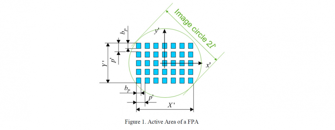
Historically, the reduction in the pixel pitch of detectors has been used to reduce the cost of the detector. This means that the number of pixels has remained constant, to give a smaller physical dimension of the detector. This can be seen by looking at the most common detector format. Over the past 20 years this has clearly been the QVGA detector (320x240 pixels or similar). The size of the active area of a detector is easily calculated once the size of the pixel and the number of pixels are known (see figure 1)[3]. Since the active area determines how many devices can be placed on one Silicon wafer, and the cost to manufacture a wafer full of devices is largely fixed, independent of the number of devices on the wafer, it is clear that the active area largely defines the cost per device. In the last 20 years the size of the active area of the detector has reduced from 16mm x 12mm for a 50 micron pixel pitch QVGA detector to 3.84mm x 2.88mm for a 12 micron pixel pitch QVGA detector. This alone implies seventeen times as many detectors per wafer and an equivalent reduction in price per detector. Naturally there are many other factors which need to be taken into account, for example, it is expected that the size of the wafer has increased and manufacturing efficiency and yield have also improved.
The result is that today, the cost of the detector and the cost of the lens assembly are the same order of magnitude, which makes the cost of the lens significant in determining the system price. Therefore, we will consider the impact of the changing pixel pitch on the lens specification and design.
We define the new camera, with a smaller pixel pitch detector, in terms of the old camera. We require that both the new camera and the old camera give the same image to the user. We assume that the number of pixels remains constant and that the field of view of the new camera is the same as the old camera. We will also assume that detector efficiency remains constant.
With these assumptions, simple trigonometry allows us to calculate that the focal length is proportional to the pixel pitch. Figure 2a and 2b shows the equivalent 17 micron and 12 micron pixel pitch systems. We see that the focal length is reduced and we can calculate that the relationship is:

Interestingly, since we defined that the camera level performance must remain the same, we must collect the same amount of energy from the object. This means that the physical aperture is invariant and so the lens assembly is faster. The f/number must decrease in the same ratio as the focal length. To give a real example, if the 17 micron camera system required a 50mm f/1.4 lens, we calculate that the 12 micron camera system will require a 36mm f/1.0 lens
The requirement to maintain the same image sharpness demands the same increase in aperture. In this waveband all the normal lenses can be considered to be effectively diffraction limited and therefore the width of the PSF is:

Where D is the diameter of the aperture of the optical system. Since λ is constant, the width of the PSF is proportional to f’/D which is the f/number. Since we require the image sharpness to remain constant as the pixel pitch decreases, we require the f/number to scale with the pixel pitch. Once again this requires that our nominal 50mm f/1.4 lens becomes a 36mm f/1.0 lens. This is shown schematically in figure 2c.
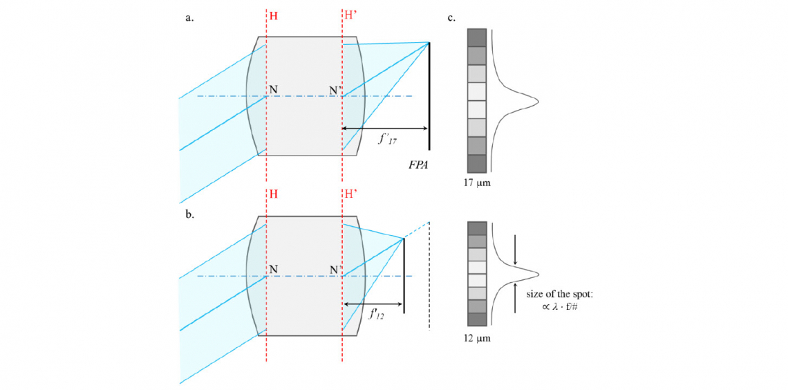
Figure 2. Schematic representation of equivalent lenses for a. 17 μm-pitch detector and b. 12 μm-pitch detector displaying the same number of pixels. H and H’ are the principal planes. c. Schematic representation of the intensity distribution of the PSF
Another, more practical way to look at the requirement for image sharpness would be to use the Nyquist limit of the detector. The image sharpness of the lens can be characterized by the Modulation Transfer Function. The Nyquist limit of the detector is defined by the pixel pitch of the detector as:

Where 𝑏𝑝 is the pixel pitch as defined in figure 1. We can define the image sharpness requirement as a constant MTF at the Nyquist frequency. So, as the pixel pitch shrinks, the Nyquist Limit increases. In the example, it increases from 29.4cy/mm to 41.7cy/mm. Since the lens performance is essentially diffraction limited, there is only one way to increase the MTF of the lens so that it remains constant for the higher spatial frequency. That is to make the lens faster in the ratio of the change in pixel pitch.
Therefore, we see two effects on the lens design as pixel pitch reduces. The first is a shorter focal length, the second is a fixed aperture size which gives a faster lens. The benefit of a shorter focal length is that it normally leads to a more compact system. This is especially true for narrow and medium fields of view. In these applications, the length of a narrow field of view lens is approximately equal to the focal length and a typical camera core is 30mm long. So for our example system the length of the camera and lens for the 17micron pixel pitch detector might be 80mm, while the 12micron pixel pitch system might be 66mm, a substantial reduction. The effect of the faster f/number is more subtle. For all fields of view we can expect the design task to become more demanding. For narrow fields of view this will be expressed in terms of difficulty to manufacture, however, for wide fields of view we can expect that the number of lens elements increases and that this will sometimes lead to an increase in the size and weight of the system.
3. FASTER OPTICS AND SYSTEM IMPLICATIONS
In the previous section we defined a requirement for a fixed aperture size as the focal length reduces with pixel pitch. This is to give identical performance at a system level. It is interesting to take a step back and consider the choices made in real world systems. It is important to choose an example where the system demands have remained consistent over the period we consider for the detector evolution, some 15 to 20 years. One example is commercial automotive night visions systems. The system requirements for this have remained effectively constant. The detector is a QVGA (320 x 240 pixels) detector and there have been three different versions as the pixel pitch has reduced. The first generation used a detector with 38 micron pixels, the second 25 micron pixels and the third generation uses 17 micron pixels. The field of view changed between the first and second versions, but all three systems have a comparable field of view. The focal length and f/number of the optics changed with the pixel and pitch and it is these changes that we will look at.
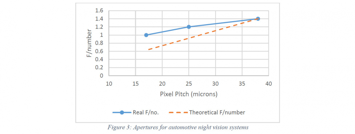
The evolution of f/number with the pixel pitch is shown in figure 3. The dashed line shows the theoretical requirement to keep the image sharpness and energy collection, while the solid line show the actual choices made by the system engineers. It is immediately clear that the systems engineers have consistently chosen to compromise the specification of the optics in order to achieve wider system goals. In the automotive environment, the critical factors are performance, cost and size. Weight is less important for this application, but, weight reduced as the size reduced.
The variation in aperture of the real system compared to the theoretically identical system means that the energy collected at the detector drops systematically and significantly between the generations. The second generation, with a 25 micron pixel pitch, collects 73% of the energy collected by the first generation (38 micron pixel pitch). The third generation, with a 17 micron pixel pitch, collects 51% of the energy collected by the first generation. Since the quoted detection range for the system remained constant for all three generations, the energy reduction has been compensated by improved sensitivity of the detector and improved image processing in the camera.
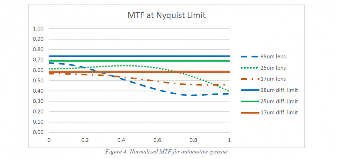
Figure 4 shows the normalized MTF vs field angle for the three lens designs used for the three different detectors. The straight lines show the diffraction limit for each of the three systems, and it can be seen that the decision to compromise the aperture results in a 20% drop in maximum performance. The dashed lines show the nominal performance of the lenses and they demonstrate that the actual image sharpness is similar for all 3 systems. When the MTF is averaged over the field of view, the image sharpness in both the second and third generation actually improves compared to the first generation. However, peak image sharpness was achieved in the second generation (+21%) and the third generation drops back to a 5% improvement over the first generation.
The improvement in the second generation was due to increased sophistication in the optical design and improved manufacturing methods. These two factors worked together because the improvements implemented in manufacturing allowed a design that was more demanding to make and included tighter tolerances. The third generation solution continued that improvement in design sophistication and manufacturing methods. In the third generation every surface was aspherised, and manufacturing tolerances again increased. Figure 4 shows that with each generation the design gets closer to diffraction limited which defines the maximum imaging performance. We can calculate a figure of merit for imaging performance, σ, where:

Using these formula, σ = 66% for the first generation, σ = 85% for the second generation and σ = 88% for the third generation. A system is normally considered diffraction limited if the wavefront error is less than a quarter of a wavelength. A quarter of a wavelength of wavefront error gives σ = 80%, so, it can be seen that the second and third generation optics are already substantially better than this conventional definition of “diffraction limited”.
With the current move in the market to detectors with a 12 micron pixel pitch a fourth generation system is now possible. There is currently no fourth generation automotive product available in high volume production, and so it is interesting to speculate what a fourth generation system could look like. We can postulate that the image performance might get even closer to the absolute diffraction limit, but it is already clear that there is limited possibility for improvement in this area. For the purposes of this exercise we can assume that in the fourth generation σ = 90% can be achieved. If we assume that the system requirements are constant, then the focal length will be defined to capture the same field of view, the number of pixels remains constant and the only remaining variable is the aperture of the system.
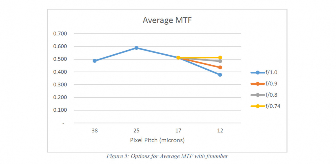
Figure 5 shows both the long term trend for average MTF over the previous 3 generations, and, the effect on average MTF of choosing different apertures for the next generation of 12 micron pixel pitch cameras. These figures are theoretical, calculated from the diffraction limit at the Nyquist frequency and the nominal value of σ = 90%. A design study for the f/1.0 case shows that a two element solution is possible, but that within the limits of two elements the maximum value of sigma that can be achieved is σ = 85%. As the aperture becomes faster the maximum value of sigma drops quickly and an additional element becomes necessary to control the optical aberrations. Although a design study for the f/0.74 case was not completed, it is quite possible that this would require 4 or more elements to adequate control aberrations. The system designer is left with a difficult choice, either compromise image sharpness or accept increased cost in the lens assembly.
An important part of the decision process in choosing the appropriate f/number will be the energy budget for the system. This is also a difficult area for the systems designer, since there is no significant improvement in sensitivity for the 12 micron detectors. For example, FLIR quote an NETD of 60mK for their 17 micron commercial camera series and 60mK for their equivalent 12 micron camera series. If we keep the f/number constant we have already demonstrated that we reduce the energy arriving at the detector. This will reduce the sensitivity of the camera to temperature differences in the scene and potentially reduce the maximum range of the camera. Clearly, this also pushes towards faster and more expensive optics.
4. OPTICAL DESIGN SOLUTIONS
Umicore has a range of catalogue lenses designed for 17 micron pixel pitch uncooled detectors and, since 2017 they have designed and manufactured a range of lenses for 12 micron pixel detectors. Umicore uses its own materials in the manufacture of the lens elements. Predominantly this is its own chalcogenide glass GASIR® which has a number of advantages. Occasionally, Germanium is also used when this gives advantages in the optical design. This extensive design database is used to examine the broader implications of the 12 micron pixel pitch detectors.
Historically the automotive case has been a demanding application, and the requirements for aperture in the rest of the market have been less severe. Consequently the aperture of the catalogue lenses for 17 micron detectors varies from f/1.0 to f/1.5, with an average value of f/1.20. Using the theoretical analysis presented earlier this would result in a range f/0.7 to f/1.1 for 12 micron detectors. However, it is interesting, to note that the range of apertures for the 12 micron lenses is much narrower at f/1.0 to f/1.1 and the average is f/1.02. This is a further indication of the difficult decisions being taken by system engineers. The decreased range and faster average for the aperture can only be because some combination of resolution and sensitivity is limiting the performance of the system. It seems likely that the limiting factor is energy collection since other sources state that the limit to resolution in current systems is still the detector[1]. Perhaps faster optics would be desirable to improve both the energy collection and the resolution, and the cost of increasing the speed of lenses does not justify the performance benefits.
In order to understand why we are seeing this much narrower range for the f/number for the 12 micron pixel pitch detector we need to consider what the solutions are for a broader range of f/numbers. So, in this study we have considered 12 micron pixel pitch lenses for a horizontal field of view from 8° to 120° and a range of f/numbers from f/0.8 to f/1.2.
It is well known from visible optics that as the f/number becomes faster the number of optical elements required to give satisfactory performance increases. There are many examples of this but perhaps the most obvious example in the visible waveband is the design of microscope objective lenses. Our case, in the Long Wave Infrared is no exception, and we start to see this having a significant impact for the first time with 12 micron pixel pitch detectors. For the 17 micron pixel pitch VGA detectors (640 x 480 pixels), the slower f/numbers allow 2 element solutions over the entire range of fields of view from 8° to 120°. For 12 micron pixel pitch VGA detectors the situation is unfortunately different.
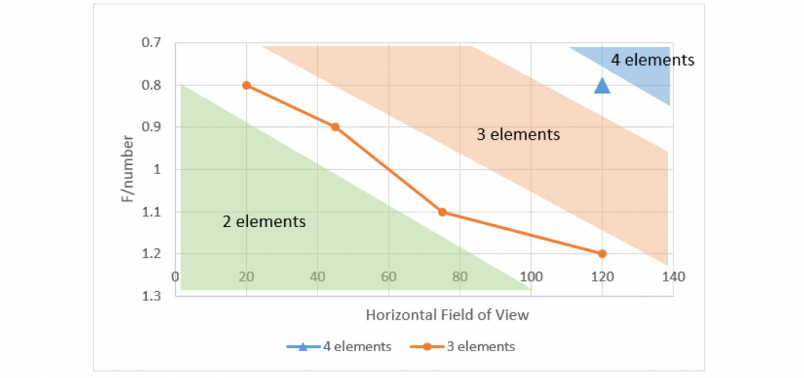
Figure 6: Graph showing the relationship between the f/number and the horizontal field of view where additional lens elements are required to provide suitable image sharpness, when the detector is a 12 micron pixel pitch VGA detector.
Figure 6 shows the f/number where an additional element is required to provide acceptable image sharpness as a function of the lens f/number. This study is based on a limited number of real design solutions and so it is not a smooth function. Nevertheless it can be clearly seen that there is a boundary line beyond which two element systems are no longer possible. The graph also shows that 4 elements are required to achieve an f/0.8 lens with a horizontal field of view of 120°. It is expected that further analysis would demonstrate that this is a point on a similar boundary line.
The point where three elements are necessary is only part of the story. One of the key elements in modern lens design is to come up with a cost effective system. In designing lenses for the 12 micron pixel pitch detectors we have seen that although a two element solution may be possible, a three element solution can be more cost effective in this boundary region. A simplistic analysis would conclude that a 3 element solution is 50% more expensive that a 2 element solution. When real design are analysed for cost it becomes clear that there are many factors that can improve the cost effectiveness of 3 elements designs. These include the possibility of smaller diameter and thinner lenses, and increased yields due to better nominal performance. For the latest generation of Umicore lenses, where the f/number is f/1.0, the introduction of 3 elements starts at a horizontal field of view of 30°.
Given that cost is such an important factor in bringing thermal imaging cameras to the market, we have looked at the manufacturing costs for a wide range of lenses. These lenses are all intended to be used with VGA detectors, and we have looked at variations in horizontal field of view and f/number as well as pixel pitches of 12 and 17 microns. Naturally the actual costs can depend upon many factors, so the costs have been normalized to allow a comparison of costs. Specifications, and therefore designs have also been modified to allow comparison, since even small changes in specification can have a large impact on cost. All costs are calculated on a like for like basis using optimized manufacturing routes available today.
In figure 7 we see the manufacturing costs as a function of f/number and horizontal field of view for a 12 micron pixel pitch VGA detector. It is perhaps unsurprising to see the general shape of curve. A narrow field of view requires a long focal length, which in turn demands larger diameter lenses. The cost of the lens assembly is a minimum around 40°, where we hit the sweet spot with minimum diameter and element count. At this point the minimum diameter of the lens elements becomes constrained by the detector size rather than by the focal length. As the horizontal field of view continues to increase the lens diameters slowly increase and the number of lens elements required comes under pressure. We found that 4 elements are required to get adequate performance at f/0.8 and 120° horizontal field of view.
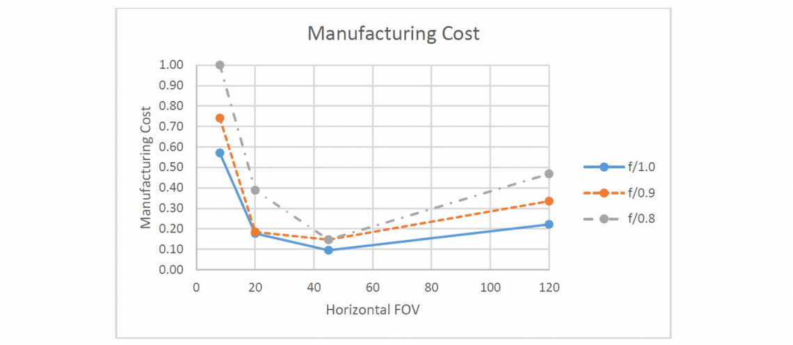
Figure 7: Manufacturing cost as a function of f/number and field of view for a 12 micron VGA detector.
We can clearly see the impact of choosing a faster f/number. The cost of an f/0.8 lens is consistently between 1.5x and 2x the cost of an f/1.0 lens. The step change between 2 elements and 3 elements accounts for the inconsistency seen for an f/number of f/0.9. However, it does indicate that for some focal lengths, a faster solution is possible, for only a nominal increase in cost.
Figure
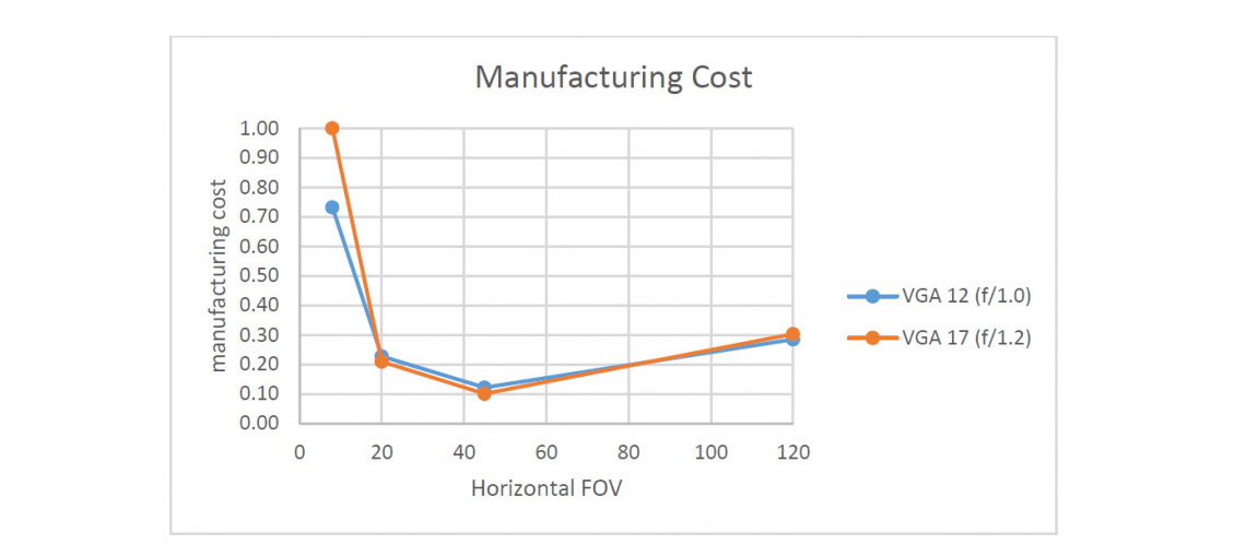
Figure 8: Manufacturing Cost as a function of pixel pitch and field of view for a VGA detector.
Figure 8 shows the manufacturing cost as function of horizontal field of view and pixel pitch for a VGA detector. Here we see the same overall shape of the curve is not changing as the pixel pitch reduces. What is interesting is that the cost savings in the lens are clearly only present for narrow fields of view. Despite the compromised f/number of the 12 micron lens assemblies, they are still marginally more expensive for 2 of the 4 examples considered.
Whether by accident or by design it appears that the f/number of the lens assembly for the 12 micron pixel camera has been chosen to keep the lens cost constant.
Taken together figures 7 and 8 give strong indications that the 12 micron pixel pitch is a turning point in camera design. For the first time like for like lens manufacturing costs do not reduce. There is continuing pressure to reduce the size of the pixel pitch further with 10 micron pixel pitch detectors available and even smaller pixel pitches proposed. Therefore, there are difficult decisions ahead for camera designers, with either further compromises required to optical performance or more expensive lenses and, perhaps, the lens assembly dominating the cost of the camera assembly.
5. CONCLUSION
We have shown theoretically that for energy collection and image sharpness the aperture of the lens is fixed and independent of the pixel pitch of the detector. Further, we have shown that this leads to a requirement for faster and more expensive lens assemblies as the pixel pitch decreases to 12 microns. In a historical real world example we have shown that system designers have chosen to compromise the image sharpness and energy collection of the optical systems. From this perspective we have looked at current optical designs for 12 micron pixel pitch detectors and examined the compromises made and the cost implications of these compromises.
This indicates that the 12 micron pixel detector is a turning point in the design of Long Wave Infra-Red camera design. Despite compromises to the performance of the lens assembly, the expected reductions in cost of the optics can no longer be delivered, except for narrow fields of view. The requirement for faster lenses lead to more complex optical designs. The combination of these two factors leads to lenses for 12 micron pixel pitch detectors which cost as much to manufacture as equivalent lenses for the previous generation 17 micron pixel pitch detectors.
The development of optical solutions for future generations of detectors with even smaller pixel pitches will be demanding. It will be necessary to consider further compromises to optical performance if the manufacturing costs are to be controlled. The computational image processing of thermal images has been steadily improving and it is possible that further developments here will allow lower performance optics and therefore lower cost optics.
REFERENCES
[1] Rogalski, A., Martyniuk, P. and Kopytko, M., “Challenges of small-pixel infrared detectors: a review”, Rep. Prog. Phys. 79, 046501 (2016).
[2] Guimond, Y., Franks, J., Bellec, Y., Bourget, A., “Umicore opens new era in IR moulded optics by opening the first high volume facility”, Proc. SPIE, Vol 5783 (2005)
[3] Schuster, N., Franks, J., “Challenges, constraints and results of lens design in 8-12micron waveband for bolometer-FPAs having a pixel pitch of 12micron”, Proc. SPIE, Vol 8704, 870424 (2013)