Molded, Wafer Level Optics for Long Wave Infra-Red Applications
The full text of this paper is available at the SPIE Digital Library.
Authors: John Franks, Umicore Electro-Optic Materials (Belgium).
ABSTRACT
For many years, the Thermal Imaging market has been driven by the high volume consumer market. The first signs of this came with the launch of night vision systems for cars, first by Cadillac and Honda and then, more successfully by BMW, Daimler and Audi. For the first time, simple thermal imaging systems were being manufactured at the rate of more than 10,000 units a year. This step change in volumes enabled a step change in system costs, with thermal imaging moving into the consumer’s price range.
Today we see that the consumer awareness and the consumer market continues to increase with the launch of a number of consumer focused smart phone add-ons. This has brought a further step change in system costs, with the possibility to turn your mobile phone into a thermal imager for under $250.
As the detector technology has matured, the pixel pitches have dropped from 50μm in 2002 to 12 μm or even 10μm in today’s detectors. This dramatic shrinkage in size has had an equally dramatic effect on the optics required to produce the image on the detector. A moderate field of view that would have required a focal length of 40mm in 2002 now requires a focal length of 8mm. For wide field of view applications and small detector formats, focal lengths in the range 1mm to 5mm are becoming common.
For lenses, the quantity manufactured, quality and costs will require a new approach to high volume Infra-Red (IR) manufacturing to meet customer expectations. This, taken with the SwaP-C requirements and the emerging requirement for very small lenses driven by the new detectors, suggests that wafer scale optics are part of the solution. Umicore can now present initial results from an intensive research and development program to mold and coat wafer level optics, using its chalcogenide glass, GASIR®.
Keywords: Wafer Optics, Chalcogenide Glass, Molded Lens, GASIR, High Volume, Thermal Imaging, Micro Lens.
1 INTRODUCTION
Wafer level optics have been around for many years in the visible waveband. Their development in cameras for mobile phones has largely driven the visible market resulting in multiple component, wafer level cameras in very high volume production. There are many advantages to wafer level optics in this context, that include tight tolerance processes to improve performance; high levels of automation for reduced cost and optimized product size to reduce the overall package size.
Optics and cameras in the Long Wave Infra-Red (LWIR) waveband are not as advanced. There are many reasons for this, the most obvious being the relatively low numbers of IR cameras being made today and the relatively large size of the arrays. However, today, we see that pixel pitches, and hence array sizes, continue to reduce and that the first mass-market products have been realized. There is a clear expectation that, where visible optics have led, IR optics will follow.
Umicore has been developing manufacturing processes for wafer lenses as part of the POLIS project. POLIS is a European Union funded, ENIAC call 9 project, it includes a work package to develop a pilot line to manufacture lenses suitable for small, high volume detectors. Umicore has considerable experience of design, molding and manufacturing of high volume lenses. It has been able to apply this knowhow to bring this development to the current state, which is detailed in this paper.
2 DETECTOR CONSIDERATIONS
As Thermal Imaging products become accepted into the consumer and industrial markets the demand for small arrays has increased dramatically. In this context a small detector is defined as a pixel count lower than QVGA, which has 320 x 240 pixels. A number of new small formats have been launched by detector manufacturers. Whereas the smallest array format used to be QQVGA (160 x 120 pixels), there are now 200 x 100; 80 x 80 and 80 x 60 pixel detectors available in the market. In the mainstream VGA (640 x 480) and QVGA (320 x 240) detectors there has been a push towards smaller pixel pitches, with the move from 25 micron to 17 micron pixels now broadly complete and a move towards 12 micron and 10 micron pixels underway. However, in the small detector space the picture is not so clear. There is a broad range of pixels pitches in the current range of small detectors, these include 50 micron, 34 micron, 25 micron, 17 micron and 12 micron detectors. Although some manufacturers have released detectors with 10 micron pixels, at the time of writing, there are no small detectors available with 10 micron pixels. Examples of formats that are currently in the market include:
- 80 x 80; 34 μm pixel pitch
- 80 x 60; 17 μm pixel pitch
- 160 x 120; 17 μm pixel pitch
- 160 x 120; 12 μm pixel pitch
- 206 x 156; 12 μm pixel pitch
The number of pixels in these examples range from 4,800 to 32,000 pixels and due to the low pixel count imaging is frequently problematic. Consequently, there are currently two routes to market for these detector formats.
The first, and currently largest by volume, is the “low cost” entry-level thermal imager. This can be stand-alone handheld units, add-ons for mobile phones or recently, thermal imagers integrated into mobile phones. In these cases, the user expects to see an image of comparable quality to those of the visible cameras. Since this standard is set by mega-pixel cameras, it is extremely demanding and a number of innovative strategies have been implemented using software and visible cameras to make the image more acceptable to the user. These applications frequently require a moderately narrow Field Of View (FOV), and most have a horizontal FOV between 20° and 50°.
The second is non-imaging applications where the image is seldom viewed and the image generated is processed by a computer to provide information from the scene. Examples of this use include people counting and industrial monitoring. In this case, the image formed only needs to be good enough to perform the desired function. In theory, these applications could have a very broad range of requirements for the FOV. However, most have a horizontal field view between 50° and 120°.
A common requirement for these two market is low system cost. The selling price for the mobile phone add-ons starts at $220 (Amazon, 2016) , and the target cost for non-imaging sensors is normally under $100. For many years, the focus of the thermal imaging industry has been on reducing the cost of the detector. Today the detector cost is similar to, and in some cases less than, the cost of the lens and so the focus has changed to include the lens.
3 DESIGN CONSIDERATIONS
The goal of low cost optics naturally drives the optical design. In the infrared, we are limited to a small range of possible materials, all of which are expensive compared to glasses that are used for visible optics. One obvious way to reduce the cost of the optical system at the design level is to limit solutions to a single optical element. While this can put severe limits on system performance for large detectors, singlet element solutions can address a surprising large range of applications and detectors.
An example of a broadly applicable single element lens is the current f=6.8 mm lens offered by Umicore (Umicore, 2016). The datasheet for this lens demonstrates that it can be used even for QVGA detectors, and depending upon the detector can give a horizontal FOV between 20° and 50°.
The way to reduce the cost of a single element lens is to reduce size and the weight. The diameter of the lens is driven by two main factors, the focal length and the f/number. For thermal imaging, the f/number must be fast in order to collect sufficient energy to produce a useful image, normally something around f/1.4 is considered a minimum and faster is desirable. So, focal length becomes the most significant variable. Conceptually, this is unusual since focal length is not normally considered a variable. It is considered a fixed parameter because the required FOV and the chosen detector define the focal length completely. However, if the FOV or the detector are considered variable, then significant cost reductions become possible. If we first consider the FOV variable, then a wider FOV will give a shorter focal length and hence reduce cost. If we consider the detector variable and require a fixed FOV, then a smaller physical size will define a shorter focal length and reduce cost. This has another positive effect that a smaller detector is normally cheaper than a larger detector. The downside of a physically smaller detector is either that we get less pixels, or that we demand smaller pixels. Fortunately, as we saw in section 2, arrays are now available with small pixels. Indeed, Umicore has seen an increasing demand for shorter focal length lenses as the pixel pitch has fallen from 50 microns to the current standard of 17 microns and we expect this trend to continue as the industry standard moves to 12 microns. Taken together these preferences and trends lead to shorter and shorter focal lengths.
4 DEFINING THE OPTICAL SPECIFICATION
Since the optical specification drives the system cost, it is important to get the specification right. Fortunately, there is a large amount of published data to help in choosing the correct specification.
Umicore was involved in the P.I.M.S (Pedestrian Injury Mitigation System) project. This was a Eureka project funded by the European Union, involving an international consortium of companies. This research project studied possible high volume, small detector thermal imagers for use in the automotive industry. In 2007, an optical design presented as part of this project (Kvisterøy, et al., 2007) showed what could be achieved with a single element solution.
Further work in 2008 (Franks, Rogers, & Guimond, 2008) demonstrated that for these sorts of applications, particularly when used over a broad range of ambient temperatures, GASIR® is a better material choice than the Germanium due to the material’s thermo-optic properties.
In 2010 as part of EU funded FNIR (Fusing Far-Infrared and Near-Infrared Imaging for Pedestrian Injury Mitigation) project, it was determined that, for the automotive application, a minimum f/number of f/1.4 was necessary (Schweiger, et al., 2010). This research supports what was an industry “rule of thumb”, and we assume that the result can be generalized to all similar systems.
With these as starting points the specification chosen was a focal length of f = 1.5mm. This can give a range of different fields of view, depending upon the detector chosen (see Table 1). The f/number should be faster than f/1.4 and the useful image circle as large as possible, in order to maximize the number of detectors than can be used with it. Similarly imaging performance should be good enough to allow use with smaller pixel pitch detectors, ideally down to 12 microns.
In order to achieve these targets in a single element, it is necessary to allow complex aspheric surfaces on both sides of the lens. Fortunately, there are manufacturing processes that allow the manufacture of these shapes on GASIR® chalcogenide glass, the material chosen for the lens. Since a fast f/number is desirable, the f/number achieved in this design is the maximum possible, consistent with the performance, size and cost targets. The resulting design achieves an f/number of f/1.2. This optical design shows that detectors are not the only things that have changed since 2007. In 2007, manufacturing considerations limited the optical performance. The current solution is designed to take advantage of progress made in current manufacturing methods (these methods are discussed later).
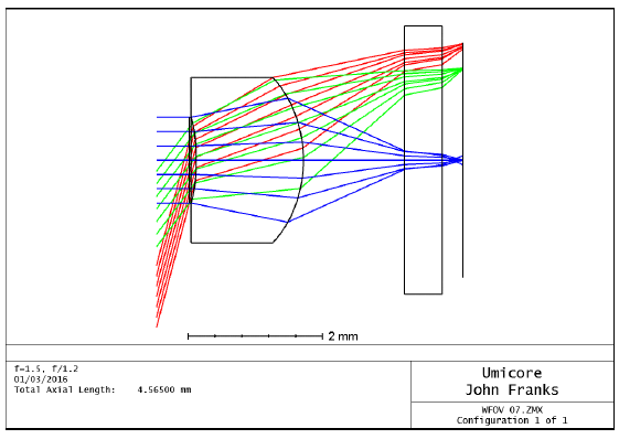
Figure 1: Optical Layout f=1.5mm
The optical layout, in Figure 1, shows a very small lens with an optical diameter of just over 2 mm. The calculated imaging performance is given in Figure 2. This shows the performance at the Nyquist limit for the three different pixel pitches in Table 1.
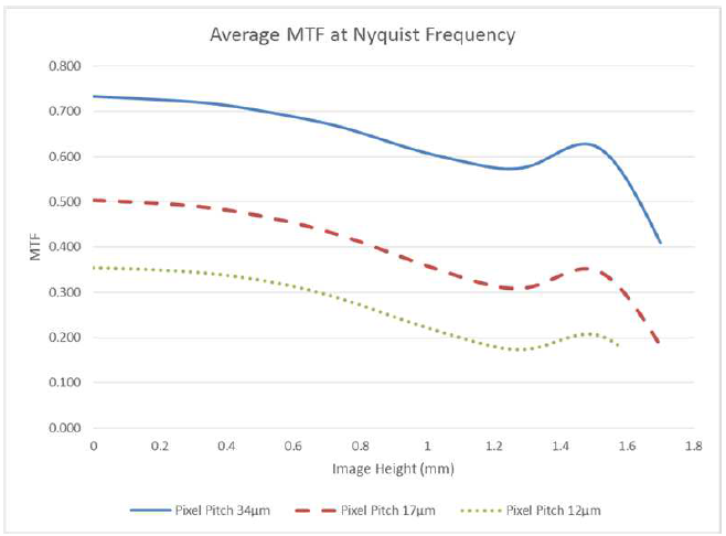
Figure 2: Calculated MTF Performance
Table 1: Field of View by Detector
| Detector Format | Image Circle Diameter (mm) | Horizontal FOV (°) | Vertical FOV (°) | Diagonal FOV (°) |
| 80 x 80; 34 μm pixel | 3.85 | 107 | 107 | Not applicable |
| 80 x 60; 17 μm pixel | 1.70 | 50 | 37 | 63 |
| 160 x 120; 17 μm pixel | 3.40 | 107 | 76 | 150 |
| 160 x 120; 12 μm pixel | 2.40 | 72 | 53 | 92 |
| 206 x 156; 12 μm pixel | 3.10 | 96 | 70 | 127 |
In Table 1 the FOV for each of the five detectors noted in section 1 is given. From this, it can be seen that this lens will function well from moderate fields of view up to extremely wide angles. It can be seen that on the detector with the largest diagonal length, the 80 x 80; 34 μm pixel detector that the short focal length combined with the large physical area of this detector, means that corners are not used. The maximum field of view is approximately 150°, which is 90% of the diagonal. The remaining 10% will be dark. Naturally, at these extreme wide angles, significant optical distortion should be expected and at 150° the optical distortion is -66%.
5 MANUFACTURING CONSIDERATIONS
It would be unusual to design a lens with no intention to manufacture it, however, manufacturing lenses this small, with complex aspherical surfaces, gives a number of problems. Conventional polishing is not possible, since both surfaces are aspheric. Conventional single point diamond turning is possible. Uniquely in materials for the Long Wave Infra-Red (LWIR) waveband, chalcogenide glasses can be molded. Conventional single or multi-cavity molding processes are possible. For lenses of this size, there is the exciting possibility of using wafer molding to produce large numbers of lenses cost effectively.
5.1 Single Point Diamond Turning
Single Point Diamond Turning (SPDT) is a very widely used manufacturing tool for LWIR lenses. A number of factors have come together to make DPT a cost effective tool for lenses in this waveband. These include:
- Low requirements for surface smoothness, due to the long waveband
- The desire to use aspheric surfaces, to reduce the number of lens elements
- Ease of SPDT machining of the most common LWIR materials
Consequently, there is a vast array of literature available on SPDT applied to infrared materials. For the purposes of this iscussion, it is sufficient to say that GASIR® can be easy machined using SPDT and that it is possible to manufacture his lens using this process. Initial prototypes of this design, and several similar designs, have been made and demonstrated using this technology.
This technology is suitable for small and moderate volumes. Each lens must be carefully placed on the machine, centered and processed, and then the entire process repeated for the second side. It is clear that this is an expensive process and it quickly reaches a point at which the costs do not reduce with volume.
5.2 Single Cavity and Multi-Cavity Molding
Molding of chalcogenide lenses has been around for a very long time and Umicore was the first company to bring high volume chalcogenide molding to the market. In particular Umicore have supplied very high volumes of molded lenses to three different automotive projects starting in 2005 (Guimond, Franks, Bellec, & Bourget, 2005). Therefore, it is natural to consider manufacturing this lens using conventional molding processes. Analysis shows that these lenses can be molded use conventional molding processes.
5.3 Wafer Molding
It has long been considered that the most efficient method of manufacturing would be to mold a wafer with an array of lenses. It is only now that this possibility can be fully considered.
Umicore has been involved with wafer molding trials for some years, however, with recent movement in the high volume market and the support of the POLIS project, it was decided that now was the time to attempt wafer molding for a specific project.
This exercise started at the beginning of the POLIS project and concluded with Low Rate Initial Production of fully molded wafers. As part of this project, we have also completed coating, dicing, singulation and testing of the lenses. Figure 3 shows a picture taken of part of a molded wafer. The wafer at this stage has been fully molded, coated on both sides and diced. The lenses at this stage are ready for assembly, and the wafer layout would lend itself to pick and place technology as used in the electronics industry. Figure 4 show a number of lenses removed from the wafer with coins to give a sense of scale.
These lenses have been tested on an MTF bench and the results are given in Figure 5. This shows the measured MTF for two lens taken from different parts of the wafer. It shows that the performance is stable across the wafer and is identical to the theoretical predictions, within the measurement accuracy of the MTF test bench.
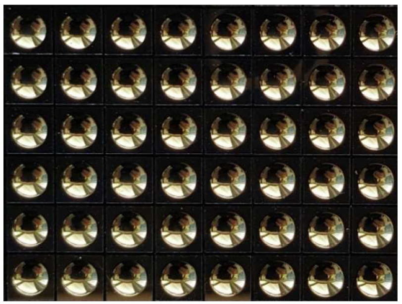
Figure 3: Section of a coated, diced wafer
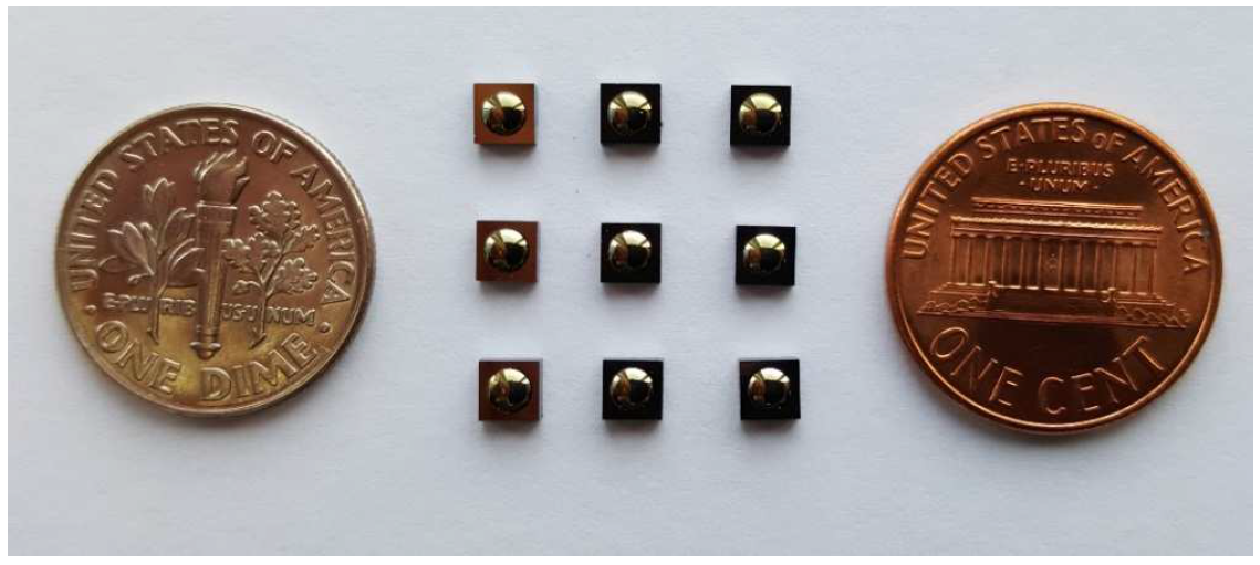
Figure 4: Singulated Lenses Ready for use
6 FINANCIAL CONSIDERATIONS
The choice of manufacturing routes depends not only upon capability but also upon costs and therefore costing tools were developed once initial feasibility had been demonstrated. These tools have been refined during the development process and updated to reflect the information coming from the manufacturing trials. One use of these tools is to determine the conditions where wafer molding could give a cost advantage, and therefore be useful.
Analysis of the variables shows that there are two key parameters. The first is the size of the lens, and for simplicity, this is defined by the diameter. The second is the number of lenses to be manufactured. The graph in Figure 6 shows the change in manufacturing cost for a 3mm lens as a function of volume. Perhaps unsurprisingly, given that there are significant tooling costs for wafer molding, wafer molding is the most expensive manufacturing method at volumes of 1000 optics. However, costs drop steeply as the tooling is amortized over a larger number of lenses and we calculate that around 10,000 lens the manufacturing cost for wafer molding is one third of the cost of SPDT and approximately the same as conventional molding. It has been demonstrated that the cost of conventional molding continues to drop as volumes increase and we calculate that wafer molding costs will reduce due to many of the same mechanisms. The continued amortization of the tooling and the cost efficiencies of handling the wafer rather than individual lenses provide additional benefits and indicate that in quantities from 100,000 units the cost to manufacture wafer molded optics could be half that of conventional molding.
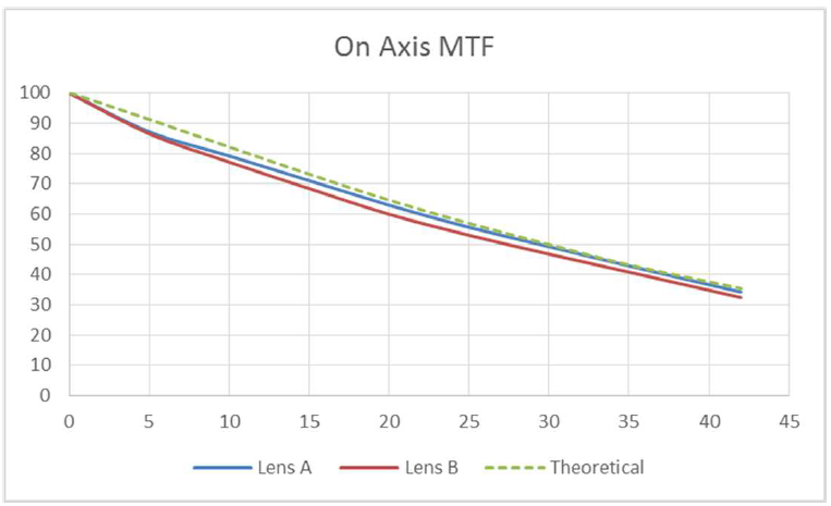
Figure 5: Comparison of Measured and Theoretical MTF
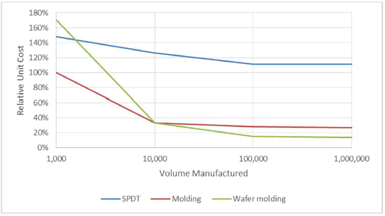
Figure 6: Manufacturing cost as a function of volume
Analysis of the relationship of cost to lens diameter for molding and wafer molding is shown in Figure 7. Applying this analysis has a higher level of uncertainty, since the diameter is only one of many physical parameters that define the manufacturing cost. The graph in Figure 7 assumes a volume of 100,000 lenses is required and several interesting things can be deduced.
- The cost of conventional molding does reduce with diameter, but flattens at smaller diameters.
- The cost of wafer molding continues to reduce dramatically as the lenses get smaller.
- For diameters above 6mm, at this volume, conventional molding is more attractive.
- For diameters below 5mm, at this volume, wafer molding is more attractive.
Deeper analysis of the models shows some of the reasons for this costing behavior. In conventional molding the final form of the lens is a disc, in wafer molding the lens is a rectangular box and this rectangular box must be larger than the disc, since it must contain the disc. Since infrared materials are expensive, at large lens diameters this becomes a cost driver. However, when the cost of the material, as a fraction of the lens cost, is calculated it can readily be seen that this is not the main cost driver for small lenses.
There are two main factors that make wafer molding cost effective. The first is the efficiency of machine usage. It is normal to consider that multi-cavity molding is more efficient than single cavity molding. This is because in the time normally taken to produce one lens, many lenses can be produced. This is more efficient in machine usage and labour costs. Wafer molding can be seen as the logical extreme of multi-cavity molding, where the maximum possible number of lenses is made in one molding process. The second factor is handling costs. With conventional manufacturing processes, each lens must be handled individually through each process following the molding (or DPT) process. Therefore, preparation, cleaning and coating becomes labour intensive. Even when low cost labor is employed, the handling costs can remain significant. By contrast, the wafer can be handled more quickly as a single item, through all subsequent processes, right up to the dicing process. Fortunately, the dicing process itself is already developed for silicon chip manufacture, is low cost and can be highly automated.
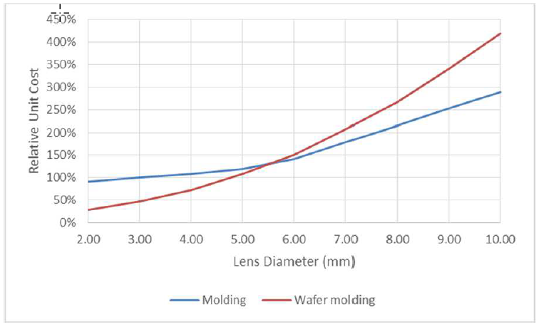
Figure 7: Manufacturing cost as a function of diameter
There has been no attempt to extrapolate to volumes above a million lenses. At this point, investment in automated handling is necessary and this was beyond the scope of this investigation. However, it is clear that automated handling solutions are already available and are widely used in visible optics. It seems likely that only minor modifications would be necessary to add IR optics to this capability.
7 NEXT STEPS
The process has been developed and the immediate next step is the manufacture of the first high volume batch of lenses. It is expected that this will be complete by the middle of this year, validating all aspects of the manufacturing process.
Beyond this, a number of things can be considered. This example given here is a single lens system; however, there are requirements for more complex multi-element solutions. Consequently, the design and manufacture of multi-element systems is part of the development road map. Should the market continue to expand as predicted, we believe that an investigation of automated handling techniques will also be required to prepare for the market of “millions” of lenses predicted by the “Optimistic Smartphone Scenario” of Yole (de Charentenay & Mounier, 2015).
8 CONCLUSIONS
We have demonstrated that wafer molding of chalcogenide glass is technically possible and that the lenses produced using this method are functionally identical to those produced by DPT and conventional molding. We have also demonstrated that wafer molding is financially attractive, given that the lens to be manufactured is of an appropriate diameter and the volumes are sufficient to justify the investment in tooling.
9 ACKNOWLEDGEMENTS
The author would like to acknowledge the work of the teams in Umicore especially those at Umicore in Olen, Umicore IR Glass in Acigné and Umicore Coatings Services in Dundee, whose hard work is presented here and without whose dedication and commitment this would not have been possible. Particular thanks are due to Priyesh Narsale, for helpful discussions during the preparation of the document. The author would like to thank the management team of Umicore EOM (Belgium) and POLIS for permission to publish. This research was supported by ENIAC call 9, project POLIS (Pilot Optical Line for Imaging and Sensing). All statements and opinions in this paper are the author’s and should not be construed as representing official positions of the EU or project members.
10 REFERENCES
Amazon. (2016, 03 01). Seek-Compact-Thermal-Imager-Android. Retrieved from Amazon.com:
http://www.amazon.com/Seek-Compact-Thermal-Imager-Android/dp/B00NYWAHHM
de Charentenay, Y., & Mounier, E. (2015). Uncooled Infrared Imaging Technology & Market Trends. Yole.
Franks, J., Rogers, K., & Guimond, Y. (2008). Optical and thermo mechanical properties of infrared glasses. Proc. SPIE 6940, Infrared Technology and Applications XXXIV, 69400P (April 15, 2008); doi:10.1117/12.779706 . Orlando: SPIE.
Guimond, Y., Franks, J., Bellec, Y., & Bourget, A. (2005). Umicore opens new era in IR moulded optics by opening the first high volume facility . Proc. SPIE 5783, Infrared Technology and Applications XXXI, 849 (June 03, 2005);
doi:10.1117/12.603756 . Orlando.
Kvisterøy, T., Jakobsen, H., Vieider, C., Wissmar, S., Ericsson, P., Halldin, U., . . . VanHulsel, A. (2007). Far infrared low-cost uncooled bolometer for automotive use. Proc. SPIE 6542, Infrared Technology and Applications
XXXIII, 65421L (May 14, 2007); doi:10.1117/12.721272. Orlando: SPIE.
Schweiger, R., Franz, S., Loehlein, O., Ritter, W., Franks J, & Krekels, T. (2010). Sensor fusion to enable next generation low cost Night Vision systems. Proc. SPIE 7726, Optical Sensing and Detection, 772610 (May 13, 2010);
doi:10.1117/12.855932. Brussels: SPIE.
Umicore. (2016, 03 01). 6.8mm Catalog Lens. Retrieved from eom.umicore.com: http://eom.umicore.com/en/infraredoptics/product-range/6.8-mm-f-1.4/