Ge for VCSELS: No epi-wafer bow
No bow in epi-wafer
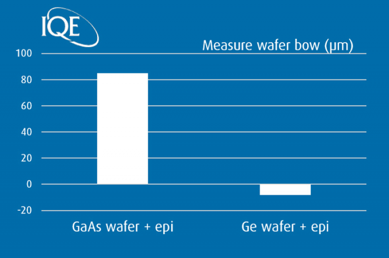
A comparison test * showed that the bow on a GaAs wafer is 10 times as high than on the Germanium wafer, 230 µm on the GaAs and 25 µm on Ge. This results in a better yield of subsequent production processes, which has a positive cost effect.

Better lattice match than GaAs
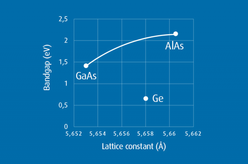
GaAs / AlxGa(1-x) As / AlAs are the preferred materials for VCSEL DBR mirrors.
As you can see on the graph, the DBR will have a slight lattice mismatch with the GaAs wafer which causes bow in the final epi-wafer.
Longer wavelength VCSEL’s are therefore difficult to make due to the need for ever thicker DBR structures to match the λ/4
As you can see on the graph, Germanium is better lattice matched to the DBR than GaAs and bow is neglectable.

Ready for longer wavelengths > 1,3µm
The lower bow makes design of safe-eye longer wavelengths >1,3µm VCSELs possible, such as long range LiDAR (>200 m)
